
Tutorial · Beginner · 28 min
8051 GPIO and Port Interfacing: Sink, Don't Source
An 8051 pin sinks ten milliamps and sources almost none. Why that inverts your LED wiring, why you write 1 before reading a pin, and what a port can drive.
Introduction
The first 8051 program everyone writes blinks an LED, and a surprising number of them do not blink. The wiring looks right, the code looks right, and the pin measures a confident 5 V doing nothing useful.
The cause is almost always the same, and it is architectural rather than a mistake: an 8051 pin is good at pulling down and bad at pulling up. Everything else in this tutorial follows from that one asymmetry—why LEDs are wired the opposite way to an Arduino, why reading a switch needs a write first, and why a port cannot drive eight of anything.
A port is just a byte
There is no GPIO API. The four ports are special function registers at fixed addresses, and writing one changes the pins:
#include <reg52.h>

void main(void) {
    P1 = 0x00;        // all eight P1 pins low
    P1 = 0xFF;        // all eight high
    P1 = 0b10101010;  // alternating
}
Individual bits get names with sbit, which is the form you will see in nearly all course material:
sbit LED    = P1^0;   // Keil C51 syntax
sbit BUTTON = P1^1;

LED = 0;              // one instruction — the 8051 has real bit operations
That ^ is not exclusive-or. It is Keil’s notation for “bit 0 of P1”. Under SDCC the equivalent comes from <8051.h> as P1_0, and the rest of the code is unchanged.
What a pin is made of
Each port pin has a weak internal pull-up to the supply and a strong pull-down transistor to ground, with the port latch driving the transistor’s gate. The two are nothing like the same strength.
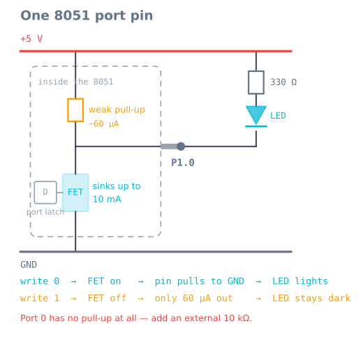
Write 0 and the transistor turns on, clamping the pin near ground and happily swallowing current from outside. Write 1 and the transistor turns off, leaving only that feeble pull-up—tens of microamps—to hold the line high. It is enough to present a logic 1 to another CMOS input, and nowhere near enough to light anything.
This arrangement is called quasi-bidirectional: the same pin is an output and an input, with no direction register to configure, because a pin holding 1 is already released enough to be driven by something else.
So LEDs go the other way round
On an Arduino you wire an LED from the pin through a resistor to ground and drive the pin high. Do that on an 8051 and you get a dim glow at best, because 60 µA is not a light source.
The 8051 wiring is inverted: anode to +5 V through the resistor, cathode to the pin. The pin sinks the current, and a 0 turns the LED on.
sbit LED = P1^0;

LED = 0;    // ON  — the pin sinks current from the supply
LED = 1;    // OFF — the pin releases the line
Size the resistor for the current you want, remembering the pin itself drops roughly half a volt while sinking:
R = (Vsupply − Vf(LED) − Vpin) / I

red LED at 5 mA :  (5 − 2.0 − 0.5) / 0.005 = 500 Ω   → use 470 Ω
red LED at 10 mA:  (5 − 2.0 − 0.5) / 0.010 = 250 Ω   → use 270 Ω
The port current budget nobody mentions
Per-pin limits are only half the story. The AT89S52 datasheet specifies both, and the second one is far more restrictive:
| Limit | Value |
|---|---|
| Maximum sink current per pin | 10 mA |
| Maximum total for all of Port 1, 2 or 3 | 15 mA |
| Maximum total for all of Port 0 | 26 mA |
| Maximum total across the whole chip | 71 mA |
Read that middle row again. A single pin may sink 10 mA, but the whole of Port 1 may only sink 15 mA between all eight pins. The classic exercise of wiring eight LEDs to a port and running a chase pattern is fine—one LED at a time. Turn all eight on at 10 mA each and you are asking for 80 mA from a port rated for 15.
Out-of-spec parts do not usually explode; they sag. Your logic levels drift, the chip warms up, and behaviour turns intermittent in ways that look like software bugs. If you want eight LEDs bright and simultaneous, the fix is a driver: a ULN2803 Darlington array sinks half an amp per channel, and the 8051 just tells it what to do.
At the port’s own limit, eight simultaneous LEDs get about 1.9 mA each. A modern high-efficiency LED is perfectly visible at that, so a chase or a bar graph is fine—just do the arithmetic before assuming brightness.
Reading an input: write 1 first
Because the same transistor serves both directions, an 8051 pin can only be read as an input if its latch holds a 1. With a 0 latched, the transistor is clamping the pin to ground and every read returns 0 no matter what is connected.
sbit BUTTON = P1^1;

void main(void) {
    BUTTON = 1;               // release the pin — REQUIRED before reading
    while (1) {
        if (BUTTON == 0) {    // switch wired to ground: pressed reads 0
            // handle press
        }
    }
}
Skipping that first line is the most common 8051 input bug. It is not a mistake you can make on a chip with a direction register, which is exactly why it catches people arriving from AVR or PIC.
Switches are wired to ground, not to the supply, for the same reason the LEDs were inverted: the weak pull-up is the idle state, and the switch’s job is to overpower it by shorting the pin down.
Port 0 is the exception
Port 0 has no internal pull-up at all. It is open-drain, because it doubles as the multiplexed address and data bus for external memory. Used as general-purpose I/O it can pull a pin down and can otherwise only float.
Fix it with an external pull-up on every P0 pin you use—10 kΩ to +5 V, or a resistor network if you need all eight. Without them, P0 outputs never reach a high and P0 inputs read noise. Ports 1, 2 and 3 need nothing.
Debouncing, because a switch is not a switch
A mechanical contact bounces for a few milliseconds, and an 8051 polling loop is fast enough to see every bounce as a separate press. The cheap fix is to confirm the reading after a delay:
sbit BUTTON = P1^1;

bit pressed(void) {
    if (BUTTON != 0) return 0;    // not pressed
    delay_ms(20);                 // let the contact settle
    return (BUTTON == 0);         // still down? real press
}
Twenty milliseconds comfortably outlasts the bounce on a tactile switch and stays far below the point a human would notice. A blocking delay is fine while you are learning; once a timer interrupt is running, sample the switch from that instead so the delay stops stalling everything else.
When it goes wrong
- The LED glows very faintly. It is wired Arduino-style, from pin to ground. Turn it around: anode to +5 V through the resistor, cathode to the pin, and drive the pin low.
- An input always reads 0. The pin’s latch is holding 0. Write a 1 to it before reading.
- Port 0 does nothing. No external pull-ups. Add 10 kΩ to +5 V on every P0 pin in use.
- One press registers as three. Contact bounce. Confirm the reading after ~20 ms.
- Everything works until several outputs are on at once. You are over the 15 mA port budget. Move the load to a ULN2803 or cut the per-LED current.
- Pins behave oddly only when the serial port is running. You are using P3.0 or P3.1, which are RXD and TXD. Port 3’s alternate functions take priority over your plans for them.
Explore the graph
Part of these builds
Projects and learning paths that include this tutorial.
Further reading