
Tutorial · Beginner · 30 min
8051 Architecture: Pins, Memory Map, and Registers
What the 8051 actually contains: a Harvard core, four ports with different personalities, 256 bytes of RAM, and a machine cycle you can count against.
Introduction
Most microcontroller courses open with the 8051, and most students meet it as a list of facts to memorise: four ports, 128 bytes of RAM, two timers, six interrupts. Memorised that way it is forgettable. Understood as a set of deliberate trade-offs made in 1980—when RAM cost real money and a chip had to fit in 40 pins—it explains almost everything about how small microcontrollers still work today.
This is the architecture tour: what is inside the package, how the memory is carved up, and why the timing arithmetic is unusually easy. The two follow-ups cover driving the pins and generating PWM from a timer.
“8051” is a family, not a chip
Intel introduced the MCS-51 in 1980 and then licensed the core widely, so nobody buys an Intel 8051 today. What you buy is a compatible part—overwhelmingly Atmel’s (now Microchip’s) AT89S52, which adds flash memory you can reprogram over four pins instead of the UV-erasable ROM of the original.
The differences worth knowing:
| 8051 (original) | AT89S52 (what you have) | |
|---|---|---|
| Program memory | 4 KB ROM | 8 KB flash |
| Internal RAM | 128 bytes | 256 bytes |
| Timers | 2 | 3 |
| Interrupt sources | 5 | 6 |
| Programming | Mask ROM at the factory | In-system, over SPI pins |
Everything else—the instruction set, the ports, the register layout, the timing—is identical. Course material written for the 8051 applies unchanged to the chip on your desk.
What is inside the package
One 40-pin DIP holds a complete computer: an 8-bit CPU, program flash, data RAM, three timer/counters, a full-duplex serial port, an interrupt controller, and four 8-bit I/O ports. There is no operating system and nothing running but your code.
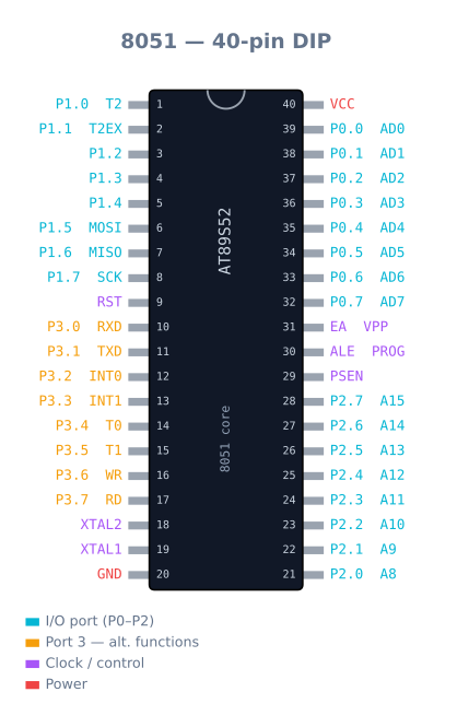
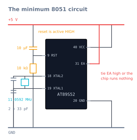
Four pins are not I/O at all and all four must be right before anything runs: XTAL1 and XTAL2 for the crystal, RST for the reset network, and EA to choose internal or external program memory. Get EA wrong and the chip does nothing, silently.
Harvard: code and data are different worlds
The 8051 keeps program memory and data memory in separate address spaces. An address of 0x0030 means one thing to an instruction fetch and something entirely different to a data access—they are different memories, reached by different instructions.
This is why C compilers for the 8051 make you think about storage classes that other platforms hide. A string literal you never modify belongs in code memory, where there are kilobytes to spare. Put it in data by accident and it eats the 256 bytes you needed for everything else:
// In code (flash) — costs nothing from your 256 bytes of RAM.
const char code banner[] = "Line follower v1";

// In RAM — 17 of your 256 bytes, gone, for a string that never changes.
const char banner_bad[] = "Line follower v1";
On an Arduino this distinction is what PROGMEM exists for. On the 8051 it is not an optimisation, it is the difference between a program that fits and one that does not.
The internal RAM map
The 256 bytes of internal RAM are not a flat scratchpad. They are divided into regions with different abilities, and knowing which is which is most of what the memory map is for.
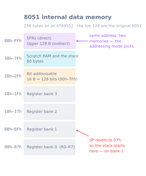
00h–1Fh — four register banks. R0 through R7 are not fixed locations; they are a window onto one of four 8-byte banks, selected by two bits (RS0 and RS1) in the program status word. Switching banks is a two-bit write, which makes it a very cheap way to give an interrupt its own registers instead of pushing and popping eight of them.
20h–2Fh — bit-addressable. These 16 bytes are also addressable as 128 individual bits, 00h to 7Fh. The 8051 has real single-bit instructions—SETB, CLR, JB, JNB—so a flag here costs one bit and one instruction rather than a byte and a mask. This is why 8051 C compilers offer a bit type that exists nowhere else.
30h–7Fh — scratch and stack. Eighty bytes for your variables and your call stack, and this is the resource you actually run out of.
80h–FFh — two memories, one address range. Direct addressing here reaches the special function registers; indirect addressing (through R0 or R1) reaches the upper 128 bytes of RAM. Same numbers, different memories, selected by which instruction form you use. On the original 128-byte 8051 the upper RAM simply does not exist.
Special function registers are just memory
Every peripheral on the 8051 is controlled by writing bytes to addresses in the 80h–FFh direct range. There is no API—there is a register, and setting a bit in it changes what the silicon does.
| Register | Address | What it controls |
|---|---|---|
P0 P1 P2 P3 |
80h, 90h, A0h, B0h | The four I/O ports |
TMOD |
89h | Timer 0 and 1 mode selection |
TCON |
88h | Timer run bits and overflow flags |
TH0 TL0 TH1 TL1 |
8Ch, 8Ah, 8Dh, 8Bh | Timer count registers |
SCON SBUF |
98h, 99h | Serial port control and data |
IE IP |
A8h, B8h | Interrupt enable and priority |
PSW |
D0h | Flags, and the register-bank select bits |
SP |
81h | Stack pointer |
Writing P1 = 0x0F; in C is a store to address 90h, and eight pins change state. That directness is the whole appeal of the chip as a teaching device.
Timing you can count
One machine cycle is twelve oscillator periods on a classic 8051 core, and most instructions take one or two machine cycles. That fixed ratio means you can calculate execution time exactly rather than measuring it:
machine cycle = 12 / f_osc

at 11.0592 MHz : 12 / 11 059 200 = 1.085 µs
at 12 MHz      : 12 / 12 000 000 = 1.000 µs
A three-instruction loop of single-cycle instructions at 11.0592 MHz takes 3.26 µs, every time, with no cache, no pipeline, and no interrupt jitter beyond what you enable yourself. Very few modern processors let you reason like that, and it is why the 8051 survives inside timing-critical peripherals.
Why the crystal is 11.0592 MHz
That number looks arbitrary and is not. The serial port derives its baud rate by dividing the machine-cycle clock, and 11.0592 MHz divides down to standard baud rates exactly:
baud = f_osc / (12 × 32 × (256 − TH1))

11.0592 MHz, TH1 = 253 :  11 059 200 / (12 × 32 × 3) = 9600.0   ✓ exact
12 MHz,      TH1 = 253 :  12 000 000 / (12 × 32 × 3) = 10416.7  ✗ 8.5% off
A UART tolerates a few percent of error; 8.5% garbles every frame. If your 8051 board prints rubbish over serial, look at the crystal before you look at your code.
What the 8051 does not have
Two absences shape every 8051 project, and neither is obvious from a feature list:
- No analog-to-digital converter. Reading a potentiometer, a thermistor, or an analog line sensor needs an external ADC chip such as the ADC0804. There is no
analogRead()to reach for. - No PWM hardware. Nothing on the chip generates a variable-duty waveform. Dimming an LED or setting a motor speed means building PWM out of a timer interrupt yourself, and paying for it in CPU time.
An Arduino Uno has both built in. That is the honest comparison: the 8051 is not a worse Arduino, it is the layer underneath one, with the conveniences removed so you can see what they were doing.
When it goes wrong
- The board is dead and nothing is warm. Check EA (pin 31) is at +5 V. Floating or grounded, the chip fetches code from external memory that is not there and executes nothing, with no symptom at all.
- It resets constantly, or never starts. Reset on the 8051 is active high. The power-on circuit is a 10 µF capacitor from +5 V to RST and a 10 kΩ resistor from RST to ground. Wiring it like an active-low reset holds the chip in permanent reset.
- Serial output is garbage. Almost always the crystal. A 12 MHz part cannot hit standard baud rates.
- Variables corrupt each other for no reason. You are probably out of the 80 bytes at 30h–7Fh, or your stack has grown down into your variables. Check your compiler’s memory map output.
- Registers change unexpectedly inside an interrupt. The stack pointer resets to 07h, so the stack starts at 08h—which is register bank 1. Either move SP in your startup code or leave bank 1 alone.
Explore the graph
Part of these builds
Projects and learning paths that include this tutorial.
Further reading